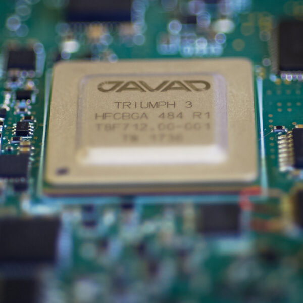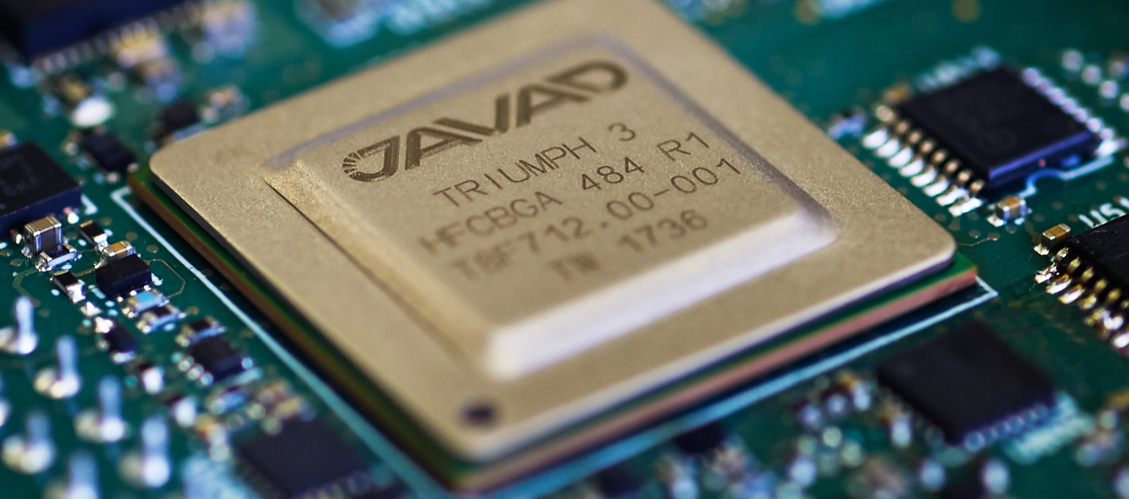
The new Triumph3 chip builds on the best features of previous generations of Triumph technology, developing a new internal structure to meet the current challenges. This new chip is based on 28 nm CMOS technology and placed in a 484-ball HFC FBGA package.
The Triumph3 chip has 864 general purpose GNSS channels and 10 additional QZSS LEX channels. Each general-purpose channel consists of 10 correlators and a memory code engine which allows receiving all existing GPS, GLONASS, Galileo, QZSS, WAAS, EGNOS, and BeiDou signals with BOC and Alt-BOC capability. The memory code engine is designed for existing truncated PN code signals as well as for future signals.
Before reaching the GNSS channels, the navigation signal goes through a sophisticated RF data processing module. This module performs digital filtering of input signals to divide the spectrum by several frequency bands (L1, L2, L5, etc). This approach allows simplifying an analog RF part along with high performance digital data processing. Moreover, this module contains two special-purpose Filters. The first is an Anti-Jamming filter based on adaptive LMS algorithm. This feature allows suppressing any multi-frequency or swapping spurious signals up to 60 dB. The second one is a classical FIR filter that is used to suppress some static interference. There are 16 identical modules for each type of filter.
The Fast Acquisition module combines four independent modules, each of which can search very long navigation signals (up to 16284 symbols) with a sensitivity of -150 dBm and run as the equivalent of 130,000 correlators.
A new RF data storage feature allows saving any GNSS signal on-the-fly to process it thereafter by CPU. In particular, this feature is used for spectrum analyzing of actual signals and interference.
To receive a navigation data of some GNSS signals like GPS L5, Galileo, BeiDou and other, the Triumph3 has several hardware-implemented data decoders. The Viterbi, Reed-Solomon, CRC, and LDPC decoders are available for this task. This decision could decrease the overall load of CPU.
The processing module of Triumph3 ASIC is based on a powerful SPARC-V8 32-bit quad core Symmetric Multi Processor (SMP) CPU combined with IEEE 754 standard 64-bit FPU. The Harvard architecture, advanced 7-stage pipeline, with branch prediction, 64 kB L1 cache, and 128-bit data access to internal memory allows exceptional performance from this processor. The total available internal memory for the CPU is 16 MB.
There are several interfaces like UART, CAN, I2C, and SPI integrated to the chip to communicate with external devices. Moreover, three PPS and three Event signals are used for external timing operations, with a resolution of about 2.5ns.
Triumph3 chip contains a very flexible power control scheme which significantly reduces the power consumption during periods when full performance is not required. The Triumph3 chip is on the front line of GNSS technology and lets us build a wide spectrum of devices.